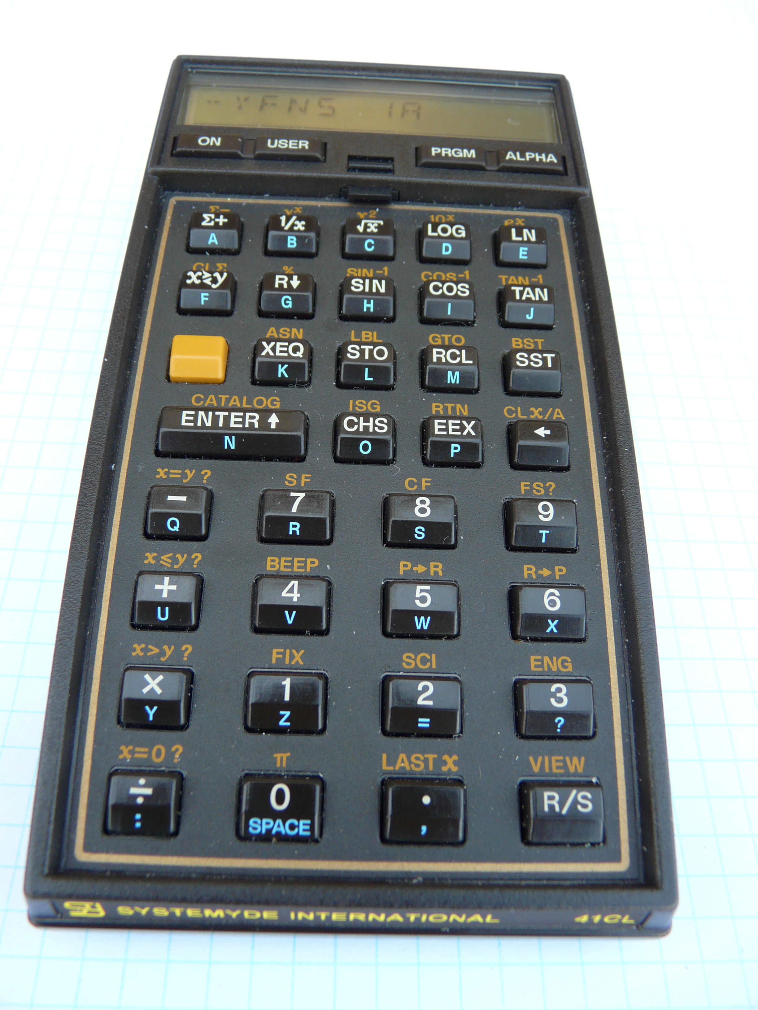
systemyde.com

NEWT Microprocessor and 41CL Calculator

[home]
[release notes]
[manuals]
[other docs]
[hardware]
[software]
[file area]
[ordering]
[contact us]
[links]
[betatest]
[Systemyde Home]
 

The 41CL takes advantage of modern technology to significantly add to the capabilities of the 41C system. The 41CL circuit board replaces the original CPU board in the calculator and provides all the features of an HP-41CX except for the Time Module. CX Time functions (the software) are included, but a Time module plugged into a Port is required for full timer functionality.

The full 600-register Extended Memory and over 120 plug-in module images are built in. Functions are included to allow these images to be virtually plugged into a calculator Port and unplugged from a calculator Port.

A Turbo mode is included, which allows the calculator to run at up to 50X normal speed.

48 empty pages (4K in length) of Flash memory are available for non-volatile storage and 58 pages of RAM are available. A sophisticated Memory Management Unit (MMU) allows full access to the large physical memory.

Full bus compatibility for the Ports is preserved, allowing the use of any peripheral designed for the HP-41 system.


02/20/2012 Status:
V3 Flash image built. Components ordered.


02/19/2012 Status:
Updated manual, covering YFNS-3A and V3 hardware, posted to site. This time around I'm not going to notify people until I actually have boards ready to ship. The stress of trying to debug boards after people had already paid was too much.


02/16/2012 Status:
Just to be clear, the Version 3 hardware does not include the timer functionality. It does double the size of both the Flash and the RAM.

I am going to try to design a separate time module replacement board. The design rules for the BGA packages are a LOT tighter than what I used on the 41CL boards, and I don't want to have to fabricate the entire 41CL board with those tighter ($$$) design rules. There isn't room on the 41CL board for all of the packages required for the timer anyway.


02/15/2012 Status:
41CL Version 3 PC board released for fabrication.

The time chip design requires three CPLDs, each in an 8mm x 8mm BGA package. A pair of XC2C256 devices and a single XC2C128. One "256" device is 95% utilized, containing channel A. The other "256" device is 89% utilized, and contains channel B. The "128" device contains the bus interface and is 75% utilized. I would use a "512" device instead of the pair of "256" devices, except that the package options are all physically too large. This is a full implementation of the HP spec except for the start/stop inputs, which are not used in the Time module. The interface CPLD can also be used wth an implementation that uses a microcontroller for the timer functionality.


02/14/2012 Status:
The version 3 board design is complete and checked. Hopefully this will be the final version. Since there are about 35 people on the waiting list, I'll probably start another batch shortly after I get the bare PC boards back.


02/02/2012 Status:
Added updated manual for YFNS-3A to the website.


01/31/2012 Status:
YFNZ-3A is almost ready to release to testing. Cleans up the error handling, removes the need for patching when loading via other than the serial port, uses the image database for the PLUG functions, automatically copies at 50x turbo, outputs a status message during long operations, etc. Will be updating the manual with the changes next. Still need to check the new board layout before sending it out for fab.


01/20/2012 Status:
The problem with the MAPEN function is hardware-related. The issue with the HEPAX DISASM function can be repaired with a simple patch. See the new "Release Notes" page.


01/14/2012 Status:
User feedback says the accuracy factor feature in the timer chip is important. That may mean no timer chip clone in a CPLD. C'est la vie.


01/12/2012 Status:
Oops, the timer chip actually requires 506 flip-flops. Trimming the accuracy factor logic, which I suspect that not everyone uses (I know that I haven't used it) means it should fit in the XC2C512, but there is no way this device will fit on the 41CL board. An XC2C384 might fit, if it replaced the current CPLD, because it comes in a TQFP144 package. But that would limit me to about 320 flip-flops. That limit would compromise the functionality.

On a more positive note, I am just about done with the circuit board modifications.


01/07/2012 Status:
The timer chip requires 326 flip-flops, which means that it MIGHT fit in a CPLD. But I don't see a way to include the functionality on the 41CL board itself. There just isn't enough room on the board for another package, especially one that is 17mm square (this is the smallest package for the biggest CPLD). So don't everyone get your hopes up.

Theoretically I could just replace the current CPLD, but the new package is BGA, which is going to mean more layers on the PC board, and my board layout tools only support up to the four layers that I currently use. Upgrading the board layout tools is expensive, so that is not likely to happen.


01/06/2012 Status:
Clone of the timer chip seems to work in the simulation. It was a nice challenge to guarantee that time is kept properly independent of deep sleep/light sleep/run state. It's interesting that the HP spec for the chip is 30 pages, but the Verilog code for the design only requires 12 pages. Now I can get back to revising the printed circuit board layout and then think about starting another batch.


12/31/2011 Status:
Almost done with a clone of timer chip. Still need to finish board layout modifications and decide whether or not to order a new board revision. I should probably start thinking about modifying YFNS to use the Image Database.


12/24/2011 Status:
48 boards have shipped. I have one board that can be soldered in place rather than using the press-fit connector. I soldered this board to my test calculator for debugging, so the connector land pattern is pre-tinned, which makes the surface uneven and unsuitable for use with the press-fit connector. Contact me if you are interested.

Started modifying the PC board layout to add a dedicated pull-down resistor so that I don't need to manually solder a jumper on the board. Considering other modifications at the same time:

1. Route two extra address lines to the Flash memory to allow for a 2x or 4x larger Flash?

2. Route an extra address line to the RAM memory to allow for 2x larger RAM?

3. Add three extra connections between the FPGA and the CPLD, just in case? This would allow one more status bit to be stored in the CPLD, which would retain the status while the calculator is off.


12/13/2011 Status:
Total of 42 boards have shipped. Slow going now because I have to notify people two or three at a time to make sure that I don't over-commit. Still seeing that one out of three people don't even bother to respond one way or the other.

Now I need to decide whether to do a build of 25 using the remaining bare boards or go ahead and revise the board to avoid soldering the jumper (hoping that I can sell more than 25).


12/11/2011 Status:
Started notifying the next people on the waiting list. There are 11 boards remaining.

The December issue of Circuit Cellar magazine has an interview of me if anyone is interested in learning what makes an IC designer tick.


12/07/2011 Status:
Caught up with orders, with a total of 33 boards shipped. 14 people didn't respond with an order, so they lost their place and the next people on the list will be notified shortly.


11/30/2011 Status:
10 boards shipped today. Invoices are out for 3 more, awaiting payment.


11/29/2011 Status:
11 boards shipped today. I hope to be able to catch up tomorrow. As with the beta boards, only about two-thirds of the people who said they were interested actually respond when I send them a link to the order form. I'll probably offer the unclaimed boards to the next people on the waiting list at the start of next week.


11/28/2011 Status:
I can only solder about 7-9 jumpers before my hand gets too shaky to be successful. So 7 boards shipped Saturday, and 9 will ship tomorrow. Plan is for another 8 or 9 on Wednesday. Then I'll be caught up.


11/25/2011 Status:
Repairing the boards requires just a single jumper. I plan to start shipping tomorrow.


11/23/2011 Status:
A single pull-down on PWO_HI should be sufficient, since this is the master reset for everything on the HP-41 bus. I was originally targeting the clocks because those signals go through vias, which are easy to solder to. But PWO_HI should be the correct fix. It's just a little harder to solder to. Will verify tomorrow.


11/22/2011 Status:
Resistors arrived today. Reprogrammed the CPLD and FPGA for half of the batch. Still need more testing on the fix, but looks good so far. I probably just jinxed everything by posting that.


11/21/2011 Status:
It may require three resistors for a guaranteed fix. Pull-downs just on PH1_HI and PH2_HI make the board start up properly 99% of the time. But I may also need one on PWO_HI for the final 1% case (where the calc has been off for a long time and the start-up delay is slightly longer). It will always start with a second press of "ON", but I haven't yet checked it with the Time module installed. Resistors should arrive tomorrow or Wednesday.

Lessons learned:
1. Just because it worked once doesn't mean it will work again.
2. Low-power design is tricky. (Duh. I already knew that.)
3. You can't fix everything with programmable logic.
4. It's good to have signals go through vias, for soldering patches.
5. Always bring unused CPLD and FPGA pins to vias too, for potential future use.
6. Always provide extra connections between the powered (CPLD) logic and unpowered (FPGA) logic.
7. The right tools (e.g. a mixed-signal sampling scope) make debugging easier.
8. Never assume. Completely test one board before programming the rest of them. (Duh. I already knew that too. Shortcuts can be fatal.)


11/20/2011 Status:
CMOS chips have an "activation" voltage, related to the transistor threshold voltages, below which nothing works. This batch of FPGAs has an activation voltage higher than that of the level shifters used to create the 41 bus signals. As a result the level shifters start operating prior to the FPGA outputs being valid. In my defense, I don't have a mixed-signal sampling oscilloscope, which would have made the problem obvious.

The addition of two pull-down resistors should solve the problem. The pull-down resistors in the FPGA don't help because they really aren't resistors, so they don't start "working" until the FPGA activation voltage is reached.


11/18/2011 Status:
Using an output from the CPLD to disable the PWO output from the FPGA during deep sleep doesn't help. That means that the problem is most likely occurring during the time before the power supplies are stable, while the FPGA outputs are supposedly "floating". Time to try the programmable pull-downs on the FPGA pins.


11/17/2011 Status:
The logic in the CPLD assumed that PWO and DPWO would not be active while the board was powering up (which is the correct behavior). I have modified the CPLD logic so that the state of these two signals is ignored during the power-up time. Now I need to try to modify the FPGA logic to somehow make the PWO output stay Low while the reset signal is active (like it's already supposed to do).


11/16/2011 Status:
This is incredibly frustrating. If I have to scrap this batch I won't
be able to afford to build another.

The thing works fine except when waking up from deep sleep. PWO
goes High for no reason, despite the fact that the reset signal is
active, supposedly holding the flip-flops static! This throws off
everything, because the entire system is synced to this edge.


11/15/2011 Status:
It would be nice if the effing FPGA would operate properly. During
power-up the reset input to the FPGA is held active for several
milliseconds after the power is stable. But this batch of FPGAs
appears to completely ignore that fact, and signals that come from
flip-flop outputs (supposedly reset) are High! WTF? This messes up
everything, because the logic assumes that a couple of these signals
really will be Low during reset.


11/10/2011 Status:
The start-up of a beta board is a thing of beauty. From zero to
full speed with nary a glitch. With this batch the start-up is a
complete mess... start-stop multiple times. Weird ISA bus timing,
PWO toggling... No wonder there's a problem.


11/09/2011 Status:
The boards are failing the final test. WTF? I guess that's what
happens when you accept orders before final test. I should know
better.

UPDATE... seems to be related to fast OFF-ON issue noticed with
the beta boards. Time to get to the root cause. Some kind of race?


11/08/2011 Status:
Flash update is taking 25 minutes per board because of the solution
books. Grrr....


11/05/2011 Status:
FPGA programmed on all boards.


11/03/2011 Status:
CPLD programmed on all boards. FPGA programming next. Flash
update image ready (unless there are more solution books).


11/01/2011 Status:
Piezo buzzers and power connections done on all boards. CPLD
programming is next.


10/29/2011 Status:
Serial connectors done. Port covers modified. Piezo buzzers and
power connections are next.


10/24/2011 Status:
First batch of 50 is back. Working on making the serial connectors.
Need to also mount the piezo buzzers and program the CPLD and
FPGA on each board, update the Flash, plus a quick final test.
Each serial connector takes about 10 minutes to make. Then another
10 minutes with the Dremel tool (using three different heads) to
modify the Port cover. Mounting the piezo buzzer and power wires
for programming is about 3 minutes and CPLD/FPGA programming
takes 5 or 6 minutes. Updating the Flash takes about 11 minutes.
Multiply by 50 boards. This is why it's taking so long.


09/21/2011 Status:
First batch of 50 out for assembly. Time to solder some
serial connectors...


09/17/2011 Status:
Added documentation for Production version. Parts for the
first batch of 50 have been ordered. We expect to have
boards available early in October.


08/06/2011 Status:
Added document describing hardware programming.


08/03/2011 Status:
Fixed the .rom files here so that no patch is required for
YFERASE and YSEC when running in Turbo mode.

Simulated fast OFF-ON sequence. All waveforms look fine.
Must be something undocumented in the timer chip?


07/22/2011 Status:
Beta status document updated with yfns .rom file patches.
Revised YFNS to revision 1E. Added files section to website.


07/16/2011 Status:
Second report of a problem with YFERASE. Until further notice
I recommend not using the flash functions.


07/15/2011 Status:
WROM instruction fix verified. Compiled logic fits in FPGA. Need
to verify on a board. Flash update image built.


07/09/2011 Status:
Revised YFNS to revision 1C. Will try FPGA update to fix WROM
instruction later today.


06/16/2011 Status:
Updated 41CL Manual to include OS register usage.


06/15/2011 Status:
The sample labels arrived. Here's what my finished 41CL looks like.


06/14/2011 Status:
The last two boards shipped today. Thank you to all of those who took
a chance and ordered one. Here is where the 21 boards found homes:
Australia (x2), Canada, Canary Islands, England, Finland, France,
Germany, Italy (x2), Norway (x2), Singapore, Switzerland (x3) and
the USA (x5). (Plus the one I kept for myself, the development board,
the two that got smoked during testing, and the two Alpha boards.)


06/13/2011 Status:
Three more boards shipped today, for a total of nineteen. Modified my
last three Port covers. Hoping to find homes for the last two boards.
Updated manual with part numbers for do-it-yourself serial connector.
Added final schematic to website for reference.


06/11/2011 Status:
One more board shipped today. First user feedback is positive. Yeah!


06/10/2011 Status:
Three more boards shipped today. Several have already arrived at their
final destinations.


06/08/2011 Status:
Three more boards shipped today. Eight remaining to go.
Created layout for 41CL label samples. Feedback welcome.


06/06/2011 Status:
Nine boards shipped today. By not responding with an order form,
five people lost their spot on the "top twenty" list today.


06/03/2011 Status:
Ten invoices sent. Will start shipping Monday! Finally, the end
of the project is in sight.


06/02/2011 Status:
Ten port covers modified for serial connectors. Should finally be
able to put away the oscilloscope, logic analyzer, power supply,
programming cables and soldering iron. :-)


06/01/2011 Status:
Flash updated on all boards (65minutes/board x 22 boards).
Twenty-five serial connectors soldered. Still need to modify Port
covers. Trying to figure out international shipping (a royal pain).


05/26/2011 Status:
CPLDs programmed on all the boards. Lost one board due to "bad id"
returned from CPLD during programming. Another $200 up in smoke.
FPGAs programmed on all the boards.


05/19/2011 Status:
The first thing I always asked a customer with a problem was "Did
you read the datasheet?" I swear I read the datasheet, but that was
a couple of years ago. Duh. I forgot that the JTAG reset signal was
active-low. So now I can update the Flash memory with the final
software. Sent the order form to the lucky 20 people who were first
in line!


05/17/2011 Status:
Still can't get the JTAG programmer to talk to the JTAG chain on the
board. Either there is something magic involved or I am overlooking
something very basic.


05/05/2011 Status:
New flash images are ready and the JTAG configuration files are all
set up. Too bad I can't get the effing JTAG programmer to talk to the
JTAG chain on the board.


04/27/2011 Status:
The Flash functions (Erase and Write) in the 41CL Extra Functions
don't work, because of a stupid coding mistake. Sorry, I'm really
a hardware guy. Now I have to find a way to make the corrections
fit. On the bright side, this should be the last of the changes to
this code, as everything else seems to work okay.


04/22/2011 Status:
41CL manual updated with changes to be applied before release.
Still need to try out revised Y-Functions in emulator.
Might be able to try JTAG reprogramming of Flash tomorrow.


04/21/2011 Status:
Piezo buzzer and power wires for programming soldered to all 23
PC boards and I only dropped the soldering iron on my leg once.
I'm sure that I'm working for Bangladesh wages on this project.


04/19/2011 Status:
New Flash image built except for revised Y-functions. Six new ROM
images and six updated ROM images. Need to finalize Y-functions
and then try to reprogram the Flash via JTAG. Cross your fingers.


04/18/2011 Status:
YGET (serial input) now works properly.
Still not sure how to test YIMP (serial block input).
Hardware issue was improper handling of register address in some
cases. Logic got broken when I modified the logic to make register
reads and writes run at turbo speed, rather than always at 1x. Oops.
JTAG programmer should arrive tomorrow. Working on generating the
configuration files necessary to try to program the flash via JTAG.
Planning on modifying Y-Functions to include a couple of new images.


04/13/2011 Status:
YGET still doesn't work correctly. More investigating.
Buffer functions work, but have to restrict to physical addresses.
Also have to restrict export and import to physical addresses.
Incredibly, something has broken User mode. More investigating.
Tired of keying in patches, so I've ordered a JTAG programmer for
the Flash memory.


04/11/2011 Status:
Found the issue with the YGET (serial read) function, and it's messy
to fix. Requires 16 more locations be patched, so I'm afraid I'll have
to do the patches myself for the boards and write the code to an open
slot in the Flash. I wish JTAG programmers weren't so expensive,
because with that I could just reprogram the Flash in one shot and
even add new images before release. Oh well.


04/09/2011 Status:
PEEKing and POKEing confirms that the serial receive hardware is
working correctly (yea!) so now I need to figure out what's wrong with
the YGET (serial read) function. I still don't know how to test the
YIMP (serial block import) function. Need to expand the manual with
the various things I've noticed, like YGET doesn't pop the fifo in the
case of an overflow, so you need to do SERINI to clear an overflow.


04/08/2011 Status:
Duh. The RS232 chip automatically shuts off with no valid level on the
RX input. Serial port transmitter works. YGET function (serial receive)
always returns indicating overflow for some reason. Investigating.


04/06/2011 Status:
Updated NEWT manual for I/O Port operation.
Serial functions need twelve locations patched. Perhaps too many?
Okay, serial port sends out of the fpga... but doesn't make it
through the rs232 driver? Transmitter sends two stop bits, which
is okay (something I forgot, obviously). Baud rate is correct, but
there are gaps between chars when running 1x, which was expected.


04/05/2011 Status:
Version 2 boards draw only 110uA in deep sleep. The changes made
from the initial version to reduce deep sleep current draw worked.
Found another bug in the serial functions. More patches to come.


04/04/2011 Status:
Updated the 41CL manual with a section on patching code.
Updated NEWT microprocessor manual for start-up delay.


04/02/2011 Status:
Well, each of the serial functions have some kind of problem. That's
the problem with using an instruction simulator to check code. Now
I could correct most of them by changing the hardware, but even if
I did that, there would still be at least one patch required. Trying
to decide which way to go... leaning towards just issuing a set of
patches, but first I need to verify the hardware.


04/01/2011 Status:
Version 2 boards now appear to be working and stable. I changed
the voltage regulators (for lower quiescent current) on version 2,
and they start up more slowly. So the start-up delay in the CPLD
was releasing reset before the FPGA power was really stable, which
led to the PWO logic not always working correctly.

Since I wasn't sure that this was the only problem, I also modified
the PWO logic to eliminate a gated clock. This means a little bit
more power, but the logic is much more tolerant of timing issues. It
also helps the synthesis and routing, as the tools seem to have a
harder time dealing with multiple clock domains.

So now I just need to go through some final checks (mainly the serial
port) before I start programming the boards for general release.


03/28/2011 Status:
Issue appears to be related to the timing of PWO and/or DPWO on
start-up. The fail cases have these signals rising with the first
edge of PH1, which isn't how the logic is supposed to work. And
it means that the display driver is out of sync with the CPU,
which explains the garbage display.


03/25/2011 Status:
Second board isn't working. Time for debug. Had to add some
circuitry to account for potential skew on the reset input.
Also corrected a couple of flip-flops that were not being
initialized by reset. These were _probably_ the source of the
start-up flakeyness, because they could lead to the turbo
control getting confused.


03/22/2011 Status:
Went through the entire design with a fine-toothed comb.
Amazing how many little things ("what was I thinking?") one
can find going back like this. Everything should be solid now.

But then the design tools decided to stop working (aborting in
the middle of a step). After a week of hair-pulling, I started
a new project from scratch in a new directory. It now compiles,
so now we'll see if it works or not. Stay tuned...

UPDATE... the new project failed to import the pin assignment
list properly (and I didn't check it) so the development board
is toast. I hope the display driver on the calculator main
board wasn't affected. Grrr... $200 up in smoke.


03/09/2011 Status:
Several of the changes made during debugging did not properly
account for clock-domain crossing. Working on fixing these.
Want the boards bullet-proof before release, so be patient.


03/05/2011 Status:
Problem occurs less often with logic recompile. WTF.


03/04/2011 Status:
The "flakeyness" that I saw in the test calculator is something
in the FPGA. About 20% of the time turning the machine on will
cause the main state machine to go awry. This never happened in
the rev 0 boards. Now, the code did change, to support internal
code for Page 5, but the code ran fine on a rev 0 board. Time
for some serious debugging.


02/22/2011 Status:
Something flakey with a Rev 1 board in my test calculator.
The Xilinx programmer fried the mouse port on my computer.
Notified of an error in one of the ROM images. Time to write
a "How to Patch Code" chapter for the manual.
Not a good day.


02/16/2011 Status:
Assembled boards are back, ready for final debug. If you have
already asked me to put your name on the "interested" list,
I'll be contacting you shortly. All of the boards are spoken for.
Remember that these should be considered "beta test" units, so
if you really don't want such a unit, let me know so that I can
offer it to someone else.


02/10/2011 Status:
41CL Calculator manual updated with photos.


01/26/2011 Status:
Finally! Out for assembly.


01/23/2011 Status:
Final version of 41CL Calculator Y-Functions source code released.


01/22/2011 Status:
All parts except the Flash memory kitted for assembly.
Manual updated describing how to use Forth image.
Final flash image is built, ready for programming.


01/14/2011 Status:
Quotes for assembly received. 41CL manual released.


01/04/2011 Status:
Bare PCBs received. One last update for Flash received.


12/18/2010 Status:
Service Module reports "CPU OK".


12/17/2010 Status:
Service Module reports "CPU BAD". Problem is with decimal mode
when inputs are greater than 9. Investigating.


12/15/2010 Status:
First production PC boards ordered.


12/13/2010 Status:
HEPAX HEPDIR command works now that WROM instruction is fixed.


12/08/2010 Status:
WROM instruction is AFU. Perhaps that's why HEPAX doesn't work.


11/29/2010 Status:
Tech manual updated. Download what is close to the final version.

HEPAX image doesn't work properly. Don't know why yet.

Board design finalized. Board #2 has been in a calculator body,
running off of batteries, for two weeks.


11/11/2010 Status:
82160A HP-IL Module seems to work. Since I don't have any HP-IL
peripherals the testing was rather cursory.

Going through the board design to try to reduce current drain.


11/05/2010 Status:
82153A Wand appears fully functional!
82242A IR Module appears fully functional!

Turns out that the IR module expects the CPU to sample the FI
bus during the second clock in a nibble time. (Undocumented)

And the Wand screech and failure during WNDTST was due to an
error in the CLRST instruction.


11/03/2010 Status:
Oops. Turns out that "WNDTST" only reports the correct data for
the first byte. Second byte is AFU in display, but correct in
the register. This one is going to be hard to find, given that
I can't use V41 to step through code. Hmm...


11/01/2010 Status:
82143A Printer appears fully functional.
82104A Card Reader appears fully functional.
82182A Time Module appears fully functional.
82153A Wand appears fully functional, but piezo element screeches
during operation. Need to investigate.
82242A IR Printer Module still reports "BAD" with TESTP.


10/28/2010 Status:
82143A Printer mostly works. "Print" button on printer does not print.
82242A IR Module prints one line, but then errors. TESTP reports "BAD".
82160A HP-IL Module not tested yet.
82153A Wand doesn't start with button press. "WNDTST" mostly
works, but causes piezo element to screech instead of beep.
82104A Card Reader doesn't start up when card is inserted, but does
"VER" on cards, and does write cards.
Time Module doesn't display continuous time with "SHIFT"-"ON".

All of this points to a problem with peripherals pulling the ISA line
High to start the calculator.

May also be issue with instructions executed during SELPRF?


10/21/2010 Status:
The flag input is active-Low, which I missed in the HP specs. I am
also sampling it during the wrong bit time...
This requires a circuit board change as well as Verilog. The HP spec
also says that the CPU precharges this signal, which I have no way of
doing as it stands right now. Investigating.


10/11/2010 Status:
82143A Printer catalogs properly, but always says "printer off".
82242A IR Module hangs the machine on start-up.
82160A HP-IL Module catalogs properly, and seems to execute, but
I have no HP-IL peripherals to verify this.
82153A Wand makes the calc start-up wierd, with high-pitched screech.
Catalogs properly, but doesn't seem to work. Also, doesn't start
calculator with press of button on wand.

All of this can probably be attributed to something wrong with the
SELPRF instruction and/or flag input


09/24/2010 Status:
Buy a copy of the October issue of Circuit Cellar magazine!
My article about the design is there.
Found a source for the CD40109 (thanks Gene), so I'll be able
to do the first production run soon.

Still have lots of things to verify though, by putting board
number 2 in a calculator body to verify operation with things
plugged into the physical ports.

Also need to build the Flash image for the release version.


08/17/2010 Status:
Deep Sleep: 310uA, Light Sleep: 4.2mA, Run: 7.9mA
Register read timing change verified.
"Loop of addition" benchmark:
1x: 1055
2x: 1913
5x: 4153
10x: 6538
20x: 9179
50x: 12022


08/14/2010 Status:
Light Sleep current drain reduced by disabling clock.
Register read timing changed to improve Turbo mode
performance. Need to verify.
First production components ordered.


08/06/2010 Status:
Investigating if it's possible to change the design to do
register writes at turbo speed, which will improve turbo
performance.
Also investigating ways to improve Light Sleep current drain.


08/02/2010 Status:
Found the light sleep current drain - floating data bus.
Deep Sleep: 330uA; Light Sleep: 6mA; Run: 7.7mA (no turbo)
Almost ready to order first production batch!


07/29/2010 Status:
Light Sleep current isn't from FPGA after all. Still looking.
Software for PEEK and POKE for I/O do bytes. Need to modify to
do words.


07/23/2010 Status:
PLUGx only works correctly with 4K modules. Software issue.
Had to delete 4-byte transmit buffer to make room for changes.


07/22/2010 Status:
User mode operation fixed. Problem was with c=regn instruction.
PLUG3 issue is a software bug.
Updated spec posted to site.


07/20/2010 Status:
User mode doesn't work. Machine hung when I tried to PLUG the
Real Estate module into Port 3.


07/19/2010 Status:
Turbo mode works!!


07/16/2010 Status:
The MMU seems to work.
Module images can be plugged into ports and unplugged from ports!
Turbo mode does not work.
Still no resolution to the power issue, but problem when eliminating
continuous reset may be due to dpwo signalling with display drivers.


07/13/2010 Status:
POKE works... just not with an on-chip peripheral address. Grr...
Eliminating continuous Reset during Light Sleep works in sim but not
in the FPGA. More grr...


07/10/2010 Status:
90% sure that Light Sleep power issue must be due to FPGA being
held in Reset during this time. Hmm...
Added option to enable/disable MMU via peripheral write. Necessary
because of error in the code in Flash. Will test next.
Verified that POKE works. Looks like block copy works.
Fixed Bank Select and Turbo state so they're preserved in Light Sleep.


07/09/2010 Status:
Still haven't found the light sleep power issue.
Corrected an issue with updating register address and PFAD
Corrected the WCMD instruction write cases, so now POKE works.
Corrected the WCMD instruction read cases, so now PEEK works.
The bank switch bits are not preserved during light sleep. Investigating.
Still haven't changed the clock to stop during light sleep.
Getting POKE to work means that I can now test the Turbo modes
and program the MMU to verify the PLUG and UNPLUG commands!


07/07/2010 Status:
Model of display chip working. Makes simulation easier. Also means
that I can build an interface to a different display. LEDs?


07/04/2010 Status:
Oops, the MMU was being disabled by light sleep. That's fixed.
Also the data bus and the isa bus were both being driven during
light sleep. Is that the source of the current drain during light
sleep? We'll see. Need to disable the clock inside the FPGA during
light sleep. That will save 5-10mA.


07/03/2010 Status:
The flag output wasn't initialized during light sleep or deep sleep.
Since the Actel flip-flops like to power-up holding a one, that
meant the output was always High until a TONE or BEEP. Not sure
how that would affect the piezo buzzer. Fixed.


07/02/2010 Status:
The problem with running programs has been found. The CLRST
was clearing all 12 bits of the ST register.


02/20/2012
© Copyright 2012, Systemyde International Corporation